Op-ed by TNO.
From broken phones to worn-out sensors: every year, the world produces more than 60 million tonnes of electronic waste. Less than 22.3% is responsibly recycled. The rest ends up in incinerators or landfills, with harmful consequences for soil, air and public health. Meanwhile, valuable raw materials are lost.
According to Stephan Harkema, programme manager for printed electronics at TNO, this needs to change. His team is working on printed electronics, a technology that radically changes the way electronics are designed and manufactured.
“This offers enormous opportunities for a new industry in the Netherlands,” says Harkema.
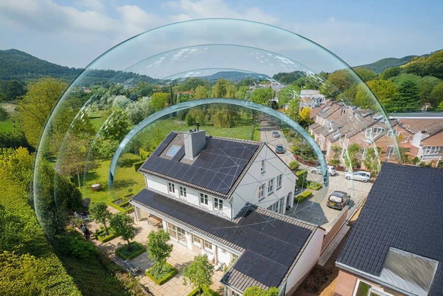
The future of electronics
Almost every device contains printed circuit boards (PCBs), made from non-recyclable plastic combined with fibreglass, copper and rare metals. TNO has reinvented that production process with printed electronics: an alternative in which layers are printed instead of etched. The result? Less material, fewer machines, no water use and far greater design freedom.
“The production process alone is already more sustainable and efficient,” says Harkema. “We use less material, no water and far fewer chemicals. At TNO, we combine this with innovations in ecodesign, bio-based raw materials and sustainable processing of plastics and metals at the end of their lifespan.
“With printed electronics, we are already making the production process itself more sustainable: less material, no water, far fewer chemicals and greater design freedom.”
The advantages of printing
Printed electronics are thin, lightweight and flexible, and can be produced in all kinds of shapes, even integrated into clothing or applied to the skin like a ‘patch’,” says Harkema.
“You can also choose different materials: copper or carbon instead of silver, and recycled plastic instead of fibreglass-reinforced plastic. This creates affordable, sustainable and eventually even compostable alternatives.”
One of the key innovations associated with printed electronics is an additional layer in the production process that makes products easy to disassemble.
“This means components can be replaced without throwing away the entire circuit,” says Harkema. “It makes repairs possible without compromising reliability or lifespan. Compared with traditional PCBs, it can deliver CO₂ savings of 40 to 50%.”
A new foundation for European industry
Many solutions aimed at reducing e-waste are only temporary fixes. Harkema sees things differently.
“Our mission is to develop technology that enables truly sustainable electronics,” he says. “Recycling is really the bare minimum. Repair, refurbishment and replacing toxic substances make an even greater impact. With printed electronics, that becomes possible. We innovate to prevent problems, not to solve them afterwards.”
Bringing new products to market is already difficult enough, especially when trying to do so sustainably and in line with ‘right to repair’ legislation.
“That is why we help companies with realistic alternatives,” Harkema adds. “Everything we develop has to be easy for businesses to apply. We have already proven this technology in automotive, lighting and healthcare. And many more applications are possible.”
“Our mission is to develop technology that enables truly sustainable electronics.”
Made in Europe
Europe is currently dependent on other countries for printed circuit boards and critical materials, making this a “huge opportunity” to bring production back to the bloc, Harkema concludes.
“E-waste contains metals worth tens of billions. Why would we throw that away, especially now that we have such a fantastic new production process? I can already see the product label: printed electronics, made in Europe.”
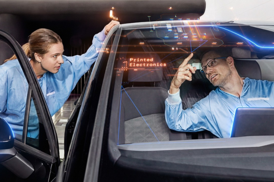
Read more here. Pictured are TNO’s Iris Kerkhof and Stephan Harkema.